
Discover the latest on Intel’s Hillsboro Oregon fab in 2026. Elon Musk tours D1X/D1D, 18A ramps with Panther Lake, 14A development, $36B+ investments, and Terafab AI chip plans. Future of U.S. semiconductors.
Intel’s Oregon facilities — the heart of the “Silicon Forest” in Hillsboro — continue to drive global semiconductor innovation in 2026. As Intel’s primary R&D and process technology hub, the D1X and D1D fabs play a critical role in developing advanced nodes like Intel 18A and 14A, powering everything from AI PCs to next-gen AI training chips.
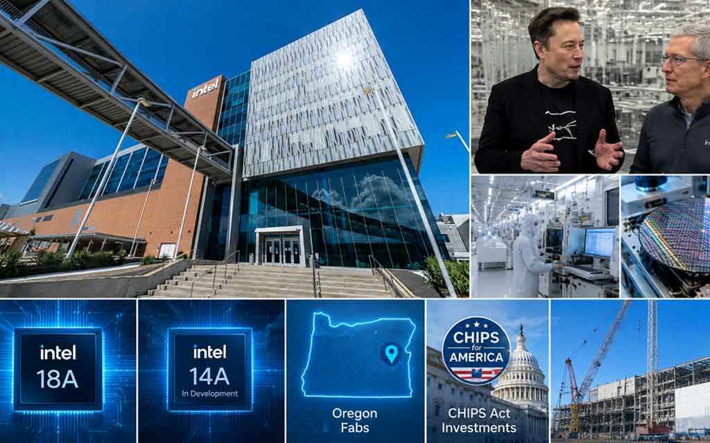
Elon Musk Tours Intel’s Oregon Fab: A Game-Changing Partnership
In a major highlight this week (May 2026), Elon Musk visited Intel’s D1X/D1D fab in Hillsboro alongside CEO Lip-Bu Tan. Musk described it as “an honor to be shown the awesome @Intel fab in Oregon” and expressed excitement for deeper collaboration with SpaceX and Tesla.
The visit strengthens Intel’s role in Musk’s Terafab project — a massive AI chip initiative targeting 1 TW/year of compute capacity in Texas for AI, robotics (Optimus), autonomous vehicles, and space tech. Intel will leverage its 18A and upcoming 14A processes. Musk and Tan were photographed holding a Tesla Optimus humanoid head, signaling strong alignment on advanced manufacturing.
This partnership boosts Intel Foundry’s credibility and highlights U.S. tech leadership amid AI demand.
Intel 18A: In Mass Production with Panther Lake
Intel 18A (1.8nm-class) has reached high-volume manufacturing. Panther Lake SoCs, Intel’s first AI PC platform on this node, are in mass production at facilities including Oregon and Arizona’s Fab 52.
Key features include PowerVia (backside power delivery) and RibbonFET transistors. Yields have stabilized in the 65-75% range for early production, with strong performance for AI workloads. Oregon engineers lead much of the development, with initial production here before scaling elsewhere.
Intel 14A: Next-Gen Leadership on the Horizon
Development of Intel 14A (1.4nm-class) advances rapidly in Oregon. This node targets risk production in 2027 and high-volume manufacturing in 2028-2029. It will be a “foundry-first” offering with higher external customer engagement.
Early PDK releases (moving toward 0.9 stage) and test chips are already with prospective clients. High-NA EUV lithography tools, first installed at Oregon’s D1X, will be key for 14A patterning. Musk confirmed plans to use 14A for Terafab scaling.
Investments & CHIPS Act Impact in Oregon
Intel has committed over $36 billion to its Hillsboro campus for modernization, cleanroom expansion (including D1X Mod3), and future nodes beyond 2025. This forms part of a broader $100B+ U.S. investment.
Under the CHIPS and Science Act, Oregon received up to $1.86 billion in direct funding for D1X upgrades, High-NA EUV, and leading-edge R&D — one of the largest single-location awards.
These funds support thousands of jobs, supplier ecosystems, and U.S. supply chain resilience.
Economic & Strategic Importance of Silicon Forest
Intel’s Oregon operations contribute billions to the state GDP annually and employ tens of thousands directly and indirectly. The site remains Intel’s global center for process technology innovation, with R&D flowing to high-volume fabs in Arizona and beyond.
Environmental initiatives include renewable energy use and water conservation, though community discussions continue around expansion impacts.
What This Means for the Future of AI and Semiconductors
The Musk visit, 18A ramp, and 14A progress position Intel strongly in the AI race. Combined with Terafab and CHIPS Act support, Oregon’s fabs are central to reducing reliance on overseas manufacturing while accelerating breakthroughs in AI, EVs, and robotics.
Last Updated: May 9, 2026
Author: Ethan Brooks– Covering semiconductor trends and future tech.


Leave a Comment